

EXPLORE SOME OF OUR PAST PROJECTS
Stamping/forging parts
-Material:silver,copper,aluminum,steel(high flexible or standard type),etc.
-Machinary:from 10T to 160T;
-Finished:sandblasting,ultrasonic cleaning;
-Au/Ni plating,painting,anodization(hardened/standard),powder coating etc;
-Applications:security products(camera,monitor…),Payment devices,home applicance;
-Measurement:3D measurement device.
Diecasting parts
-Material:ADC12(aluminum alloy) etc;
-Machinary:from 160T-800T;
-Finished:sandblasting,ultrasonic cleaning;
-Chromate plating,painting,powder coating etc.
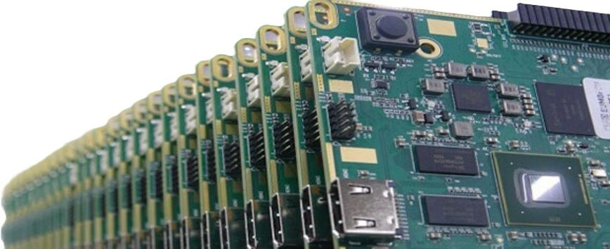
PCB assembly
– Visual inspection: general quality inspection
– X-ray test: check whether there is short-circuit cold welding or bubble problem in BGA, QFN, and another welding.
– Automatic optical detection: check whether there are false welding, short circuit, few parts, polarity reversal, etc.
– Online testing.
– Function test (according to the test steps you provided)
PCB
– Layer: from 1 to 70.
– Max board size: 2 layers: 1500*570mm, >=4layers: 570*1200mm(Need to evaluate when length is over 570mm).
– Max.array size for PTFE material(Thick<=0.5mm):16*18 inch.
– Copper thickness: from 1/3Oz to 12Oz.
– Surface finishing: HASL Lead free, ENIG, OSP, Immersion Tin, Immersion Silver, Gold plating, Tin plating.
-Gold thickness with hard gold plating: from 0.1um to 1.3um.
-Min diameter for BGA pad: 7mil.
-01

– 02

– 03
– 04
